This website uses cookies so that we can provide you with the best user experience possible. Cookie information is stored in your browser and performs functions such as recognising you when you return to our website and helping our team to understand which sections of the website you find most interesting and useful.
Irradiated Materials, Fuels and Actinides Handling and Characterisation
Technology Platform
About
Mission: To enable chemical, microstructural and mechanical property characterisation of highly active materials to further a mechanistic understanding of actinide chemistry and radiation effects on materials and underpin a safe and efficient nuclear power industry.
Capability: The Irradiated Materials, Fuels and Actinides Handling and Characterisation platform is an open-access facility for academic and industry collaborators via Royce or National Nuclear User Facility (NNUF) access schemes. Hosted at the National Nuclear Laboratory’s site at Sellafield, it consists of mainly high-activity shielded facilities at the Active Handling Facility (AHF) operating in conjunction with the high alpha and medium active laboratory facilities of Central Laboratory.
Multiple capabilities located within a heavily shielded high active cell at the Active Handling Facility (AHF), enable post-irradiation characterisation of α, β and γ highly active nuclear material using remote handling techniques. Royce funded equipment together with NNL supporting equipment provide the capability to size reduce, prepare and characterise irradiated material using optical microscopy, SEM (with EDX, WDX and EBSD), Raman Spectroscopy and small-scale mechanical testing.
High integrity alpha active gloveboxes and fumehoods are available in NNL’s Central Laboratory to analyse medium to high alpha active materials (U, Np, Pu, Am) in both solid and solution state to enable reaction monitoring, speciation and phase characterisation. Central Laboratory also hosts the Electron Optics capability that allows the characterisation of irradiated fuels and structural materials, wasteforms and other materials at length scales from the millmetre to Ångstrom. Working with industry, government and academia, we have experience of analysing materials from a variety of reactor sources, simulated and test irradiation programmes and from industrial plant using state-of-the-art preparation techniques and a range of analytical techniques. These include X-ray microtomography, SEM, FIB , plasma FIB with SIMS and (S)TEM equipped with EDX and EELS analysis systems to provide structural and compositional information on volume reduced pieces of high activity materials, from AHF, to provide an integrated offering to high activity materials analysis.
NNL has access to a large variety of material from historic waste forms to irradiated spent fuels, cladding, graphite and actinide compounds, which are available to access on request allowing a user the unique opportunity to gather a range of material property information on high active spent nuclear fuel and material.
Platform Leads
Simon Dumbill
Technology Platform Lead
Electron Optics
Simon Dumbill has over thirty-five years’ experience in the nuclear industry involved with the study of the performance of materials, especially concerning the effects of irradiation on materials. This has particularly focused on the application of electron microscopy techniques to characterise materials at high spatial resolution.
As the NNL technical lead in the area of microstructural analysis, he has wide-ranging knowledge of the application of many analysis techniques and experience of a range of materials from steels, through zirconium alloys to graphite, carbon deposits and ceramic wasteform materials. Simon has managed facility relocation projects in NNL and its predecessors and led the effort to maintain an electron optics capability in the UK nuclear industry which has culminated in the establishment of the National Nuclear User Facility and Henry Royce Institute facilities in NNL’s Central Laboratory. Growing user access to these facilities is a current theme involving links with prospective users and translating their needs into programmes.
Rebecca O’Neill
Technology Platform Lead
Hot Cell Materials Characterisation
Rebecca O’Neill is a deputy technical lead within the Post Irradiation Evaluation (PIE) capability at the National Nuclear Laboratory. She is involved in providing technical advice and support to several large, long-term projects working to provide information on fuel and reactor material performance to support the ongoing operation of the UK reactor fleet.
Rebecca’s experience is within hot cell microscopy. Primarily using microscopy to characterise irradiated material including graphite, oxide fuels, stainless steel, and zirconium cladding, for both UK and international customers. The variety of work has ranged from condition monitoring of reactor fleet material to material failure investigations. Together with projects that have provided evidence that will contribute to the decision on the long-term storage of the UK’s nuclear material.
Mark Sarsfield
Technology Platform Lead
PU Science
Mark Sarsfield is an Industrial Chemist with a PhD in inorganic chemistry, has chartered accreditation and is a Fellow of the Royal Society of Chemistry. Appointed as an NNL Laboratory Fellow within the Radiochemistry team, Mark is the technical lead on projects funded by the European Space Agency (ESA), Nuclear Decommissioning Authority (NDA), Sellafield Ltd, and the EU Framework Program VII/H2020. With a strong background in actinide chemistry, Mark provides technical support to the NDA plutonium disposition programme and THORP and MAGNOX reprocessing plants at Sellafield and is an independent technical expert on the Magnox Reprocessing Technical Committee. Mark leads a UK Safeguards programme, delivering training courses for the IAEA and provides similar training to MoD and NNL staff on the nuclear fuel cycle. He has developed an international network through participation in EU framework projects (PATRICIA, ASGARD, ACSEPT) and collaborations with US National Laboratories. Mark is a visiting research fellow at the University of Manchester and has published one book chapter and over 55 journal articles with a h-index of 24.
Equipment

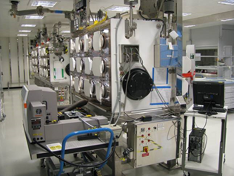
A brand new, state of the art, micro-Raman spectrometer is available for use at NNL’s Central Laboratory. The instrument is capable of analysing a wide variety of radioactive materials and liquids either in an alpha active glovebox or fumehood environment.
The glovebox is fitted with fibre optic feedthroughs to allow analysis with 514 or 785nm Compact Fibre Optic Probes (CFOPs) and can analyse high specific activity alpha materials such as AmO2, PuO2 and MOx.
The fumehood has 514, 633 and 785nm lasers with a motorized x,y,z stage and LiveTrack dynamic focusing.
Instrument Specification
Renishaw InVia Qontor Spectrometer System:
- 1 to 300 mm laser spot size depending on objective lens and laser
- 5×, 20×, 50×LWD, and 100× objectives 50xLWD objective for CFOPs
- Confocal capability
- Peltier cooled CCD array detector
- Rayleigh line rejection filter down to 50cm-1 (514nm) and 100cm-1 (633, 785nm) 150 cm-1 for CFOPS from the laser line
- Raman imaging software for univariate spectral analysis of data sets
- StreamHR software for high resolution (to < 300nm) fast Raman imaging
- Spectral search function
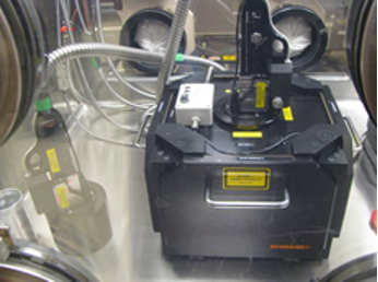
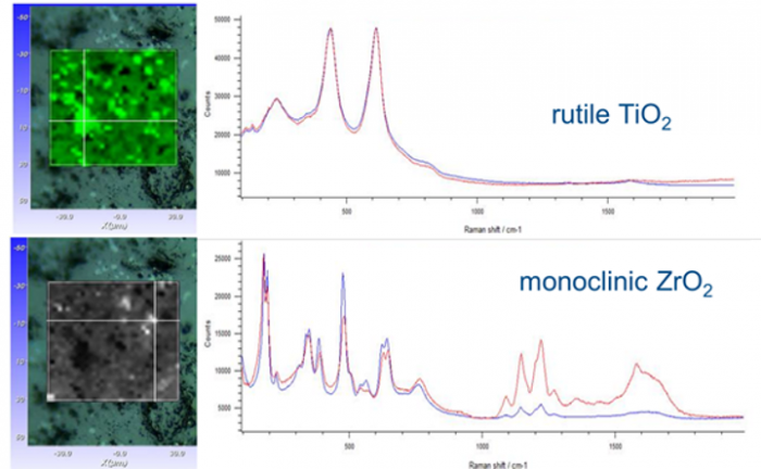

A nuclearized Olympus optical microscope with three Raman lasers and a microhardness HV tester (Vickers), is currently available for use in the non-radioactive setting of the NNL Workington Facility. It will be installed in the Active Handling Facility at The NNL Active Handling Facility.
The multiple capabilities of this microscope allow complete characterisation of highly radioactive samples, including but not limited to, irradiated fuels, cladding, graphite and waste forms, available in the Active Handling Facility, at request. The optical microscope is complemented by the three Raman lasers allowing features of interest to be visually identified, together with the chemical composition determined. Further mechanical property information can be inferred by the microhardness tester.
![]()
Instrument Specification
Optical Microscopy:
- LOM imaging – BF, DF, POL
- Resolution of >2 µm
- Six optical objectives (for imaging and positioning) at 1.25x, 2.5x, 5x, 10x, 50x, 100x
- Integrated image analysis software
Raman Spectroscopy:
- Horiba confocal system with 3 lasers:
- 532 nm/100mW air cooled laser (spatial resolution 4 µm)
- 660 nm/100mW air cooled laser (spatial resolution 4 µm)
- 785 nm/90mW air cooled laser (spatial resolution 8 µm)
- Multichannel cooled CCD
- HORIBA LabSpec 6 software
Microhardness Testing:
- Vickers microhardness tester with load range of 0.1N to 4N
Standard sample sizes: Flexibility is dependent upon specific requirements
Supporting Equipment:
Deben tensile/compression stage
Deben MT5000 MICROTEST tensile/compression stage with both a 2KN and 5KN load cell. The modules allow many different materials to be deformed and stretched at loads up to 5KN. The stage can be used for tensile testing, 3 & 4 point bend tests and compression tests.
Includes: a horizontally mounted tensile and compression stage with 2KN and 5KN load cell and a compression cage. Microtest Acquisition software is used for control of the modules and provides real-time display of force-extension curve.
Vibratory Polisher
ATM Saphir Vibro polisher with a 308 mm (inner diameter) bowl for polishing non-mounted specimens, for simultaneous polishing of up to 21 specimens. Designed for use with all polishing cloths and a lid to protect cloth from contamination.
An automatic vibratory polisher prepares specimen surfaces with very minimal deformation for applications of techniques such as LOM, SEM or TEM analysis.
Uniquely able to work with irradiated materials including fuels, NNL’s Irradiated Materials Characterisation capability has been funded from a number of sources including Royce, NNUF and EPSRC and includes the following instrumentation and facilities:
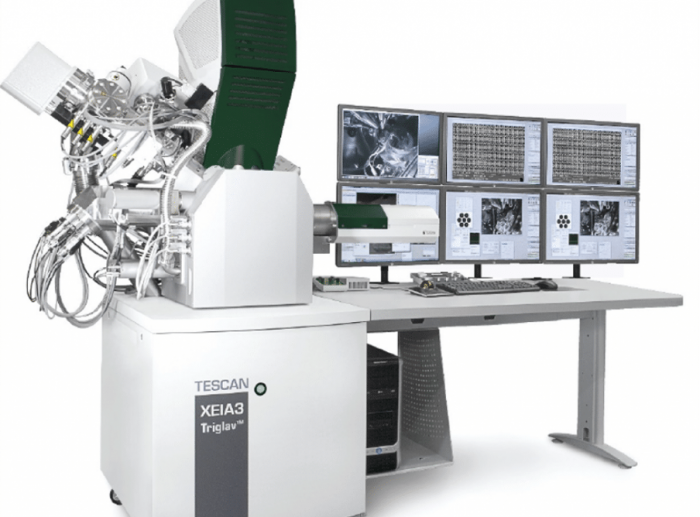
- A Plasma focused ion beam FIB-SEM with EDX, EBSD, ToF-SIMS (Tescan Xeia)
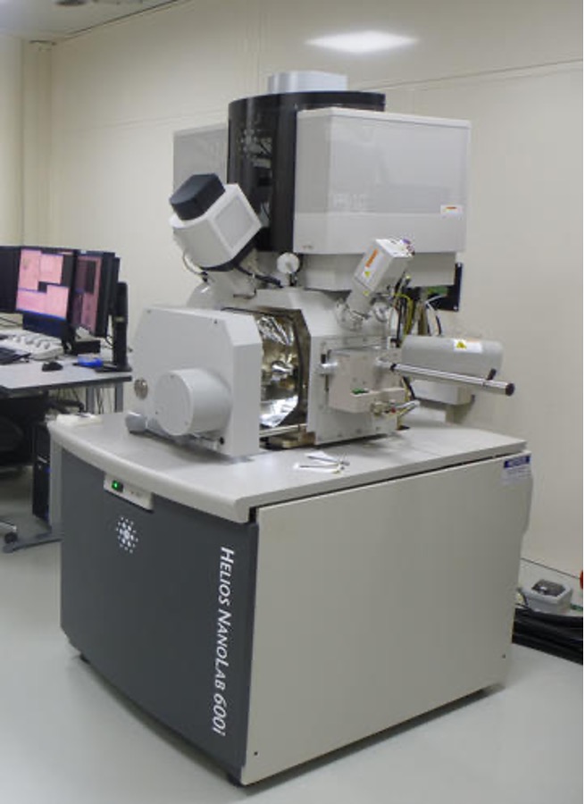
- A high-resolution FIB-SEM (FEI Helios 600i)
- A high-resolution X-ray CT capability (Bruker Skyscan 1172)
- A 200 kV (S)TEM with EDX and EELS (JEOL 2100)
- A 200 kV aberration-corrected FEG-TEM with EDX and EELS (JEOL ARM 200CF
- SEM with EDX, WDX and EBSD (Tescan MIRA)
- Hardness testing
- Sample preparation
PFIB
The Tescan XEIA PFIB is a national asset for the characterisation and preparation of active material samples in the UK. Compared to a Ga+ ion FIB, the PFIB is considerably faster (up to x 50) allowing for higher volume samples to be milled and analysed than previously possible.
The PFIB is fitted with a TOF SIMS system, capable of operating in negative/position modes – allowing for the detection of a wide variety of isotopes – including those of hydrogen. This is a first for any active FIB in the UK.
Detailed X-ray mapping and analysis is possible due the FEG electron source and two large detectors; a Bruker 60 mm2 (1 Sr) FlatQuad optimised for maximum X-ray collection and Bruker 100 mm2 main detector which allows greater flexibility with other imaging modes. Additionally, electron backscatter diffraction capability allows grain orientation mapping using a Bruker EBSD (with TKD) detector.
By combining the above techniques with the milling aspect of the P-FIB allows for unprecedented site-specific analysis and sample preparation. The acquisition of 3D datasets is greatly enhanced by the rapid milling capability. Examples of use could include: preparation of TEM lamella for radiation induced segregation analysis at grain boundaries, mapping of grains using EBSD, preparation of APT needles characterisation of zirconium oxides using SEM and many more.
Uses/Applications
- Detailed microstructural investigations into active materials, including EDX and EBSD mapping.
- Destructive 3D tomography
- TOF-SIMS isotopic analysis
- Preparation of TEM samples for export to Universities and/or NNL’s TEMs
- Preparation of APT needles for export to Universities
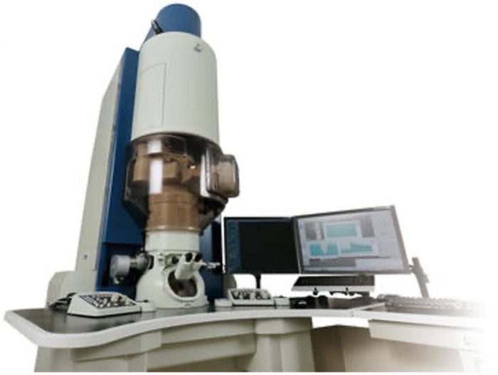
FIB-SEM FEI Helios 600i Nanolab with EDS & EBSD
A high-resolution FIB-SEM with a full complement of analytical capability is available for use at NNL’s Central Laboratory (Sellafield).
Installed in the active area of Central Laboratory on Sellafield site, the instrument combines a UHR electron microscope with energy-dispersive X-ray analysis (EDX) and electron back-scatter diffraction (EBSD) analysis, as well as an ion column for sputtering materials and preparing size-reduced specimens for TEM analysis. This FIB also includes a cryo-stage allowing the preparation of zirconium alloy samples free from hydride artefacts.
Previously the instrument has been involved in examining AGR fuel cladding, vitrified waste, uranium powders and precipitates, and preparing atom probe tomography needles.
X-ray computed microtomography – Bruker Skyscan 1172
A high-resolution X-ray CT capability is available for use at NNL’s Central Laboratory. Installed in the active area of Central Laboratory on Sellafield site, the Bruker Skyscan 1172 allows non-destructive imaging of specimens with a peak resolution of 0.9 μm.
Comprising a 100 kV, 10 W X-ray source, 11 MP CCD detector, and a micropositioning stage, the 1172 is capable of scanning samples as large as 50 mm in diameter and can perform z-stacking for particularly long specimens.
Previously the instrument has been involved in examining carbonaceous deposits, uranium foil in cement, Magnox simulant sludge, various cements and grouts.
200 kV (S)TEM with EELS capability – JEOL 2100
A 200 kV (S)TEM with EELS capability is available for use at NNL’s Central Laboratory (Sellafield site). The instrument combines the high spatial resolution of a transmission electron microscope with chemical analysis by EDS, and EELS.
The instrument is further supported by NNL’s FIB and PFIB instruments, as well as ion mill and electropolishing equipment for TEM sample preparation.
Previously the instrument has been involved in examining AGR fuel cladding, zirconium cladding, MTR fuel, and wasteforms.
200 kV aberration-corrected FEG-TEM – JEOL ARM-200CF with EDS and EELS
A 200 kV aberration-corrected FEG-TEM with EELS capability is expected to be available for use at NNL’s Central Laboratory from late 2022.
Installed in the active area of Central Laboratory on Sellafield site, the instrument is capable of sub-Angstrom imaging resolution, and atomic resolution chemical analysis by EDS (0.98 Sr Oxford Instruments X-Max 100 TLE detector), and Gatan GIF Quantum 965 ER with Dual EELS and EFTEM capabilities.
The instrument is further supported by NNL’s FIB and PFIB instruments, as well as ion mill and electropolishing equipment for TEM sample preparation.
SEM with EDX, WDX and EBSD (Tescan MIRA)
An analytical SEM with low vacuum and full analytical capability, the Tescan MIRA installed at NNL’s Active Handling Facility (AHF) Is able to characterise highly active samples prepared in the AHF or elsewhere.
Hardness testing
A Struers Duramin-40 A2 hardness tester with a versatile loading range of 10 gf to 31.25 kgf
(indent size from a few µm to hundreds of µm) is available in Central Laboratory for the testing of irradiated steels and other materials. Furnaces are available for annealing at Central Laboratory and the system has recently used to compare the hardness of irradiated and annealed variants of pressure vessel steel.
Sample preparation
Size reduction and polishing , including electropolishing is available to prepare irradiated samples for microscope examination. Damage layers resulting from FIB processing can be removed using low energy ion beam milling.