
This website uses cookies so that we can provide you with the best user experience possible. Cookie information is stored in your browser and performs functions such as recognising you when you return to our website and helping our team to understand which sections of the website you find most interesting and useful.

2D Materials
Technology Platform
About
The national Royce ultra-high vacuum (UHV) 2D materials facility combines world-leading academic research and a unique equipment suite to enable further research, prototyping and feasibility studies of 2D material-based optoelectronic devices. We address the following aims: (1) develop, study and manufacture novel 2D optoelectronic devices for key areas of UK research, such as quantum technologies and low power electronics; (2) advance the quality of 2D materials heterostructures to a technologically relevant level for optoelectronic applications; and (3) develop new, fully automated heterostructure assembly techniques for small batch production.
2D materials cover a wide range of properties from conductive to insulating, transparent to opaque, diamagnetic to ferromagnetic, and mechanically stiff to compliant. Importantly, these materials can be stacked on top of each other to form artificial solids with tailored properties, so-called van der Waals (vdW) heterostructures, offering an immense range of opportunities for new applications. Such layer-by-layer assembly is conceptually similar to molecular beam epitaxy which is ubiquitous in the semiconductor industry, however, mechanically fabricated 2D heterostructures do not require lattice matching, providing a unique opportunity for combining over 200 different 2D materials. Such heterostructures have already been shown to offer various appealing functionalities including tunnelling transistors, light-emitting diodes, photodetectors, and various sensors.
To date, the 2D material heterostructure assembly is widely adopted using various polymeric films in air and inert gases. The Royce 2D Materials Technology Platform presents a unique opportunity to perform the heterostructure fabrication in Ultra High Vacuum avoiding any contact with air or any organic matter. It is accompanied by a range of tools for characterisation, fabrication for both one-off device prototyping, and small-batch production.
Platform Lead
Prof. Roman Gorbachev
Technology Platform Lead: 2D Materials
Roman Gorbachev is a Research Professor in the Department of Physics and Astronomy at the University of Manchester (UoM). He completed his PhD in physics at the University of Exeter in 2009, and established his research group at the UoM in 2014. Prof. Gorbachev’s research area is experimental condensed matter physics with an emphasis on fabrication of nanoscale low-dimensional devices. The availability of novel nanoscale materials, such as atomically thin 2-dimensional crystals and nanowires has enabled the assembly and study of composite electronics and mechanical devices, as well as the exploration of fundamental physics in these low-dimensional systems. The use of modern state-of-the-art semiconductor device fabrication techniques and the development of new methods of material synthesis/manipulation are essential parts of Roman’s research, which enables him to explore the new physical phenomena and impact future technologies.
Equipment
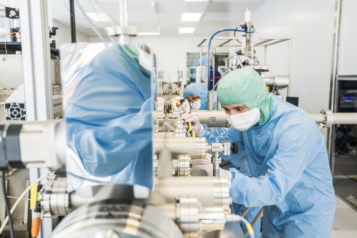
The Royce 2D Materials Technology Platform is housed in the cleanrooms with a broad range of nanofabrication and characterisation capabilities. As the largest 2DM facility in Europe, our cleanroom is tailored for nanofabrication of 2D optoelectronic devices and houses a broad range of instruments:

UHV 2D Press for 2D materials has enabled a technological leap in the quality of 2D materials and their heterostructures beyond the current state-of-the-art. This world-first UHV 2D Press integrates heterostructure assembly and characterisation at 10-10mbar pressure, comparable with industrial molecular beam epitaxy tools. It includes remotely controlled 2D crystal transfer with a 15-axis micromanipulator, lithography-free contact deposition, and device encapsulation.
![]()
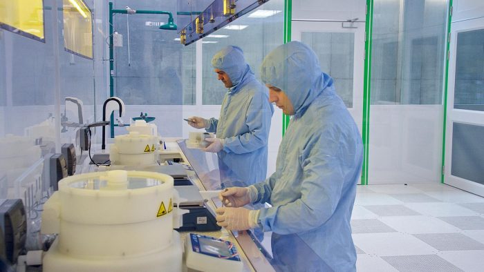
Complementary Glovebox transfer systems: for quick and less critical prototyping, two argon-filled chambers house our crystal transfer systems.

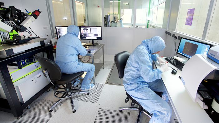
Cryogenic optical kit: Attodry800 allows cryogenic optical characterisation for 2D materials and their heterostructures fabricated in the UHV suite, and allows automated probing of the heterostructures to assess their performance and quality. It is fully integrated with the UHV 2D press allowing UHV sample transfer with no air exposure.

Cryogenic STM: RHK PanScan STM is designed to study the surfaces of 2D materials across a wide range of temperatures (8-300K) with atomic resolution, looking into samples morphology, and electronic properties and defect with atomic resolution. It also allows UHV sample transfer from other modules of the UHV suite with no air exposure.

Electron beam lithography: Vistec EBPG 5200 is industrial 100kV electron beam lithography designed to work with both small prototyping batches and larger 6” wafer scale manufacturing.

Ion beam milling: Zeiss CrossBeam Ga+ FIB milling for precise nano-machining and sculpting of various nanostructures.
Equipment

A range of deposition and etching capabilities, including Moorfield electron beam deposition and AJA UHV sputtering systems, Picosun ALD R200, Stratum PECVD, 3 Oxford PlasmaLab ICP RIE machines, and a variety of smaller tools.

Environmental Scanning Probe Microscopy: Asylum Research Cypher integrated into an argon chamber allows for atomic resolution AFM and nanomanipulation while preserving air-sensitive 2D materials.

SEM: Zeiss Ultra Field Emission SEM provides resolution as low as 1 nanometre for imaging and characterisation of 2D nanostructures.

XRD: Rigaku SmartLab X-ray diffractometer for high-resolution structural analysis of 2D crystals and laminates.

Raman Spectroscopy: Horiba system for standard sample characterisation.