


Description
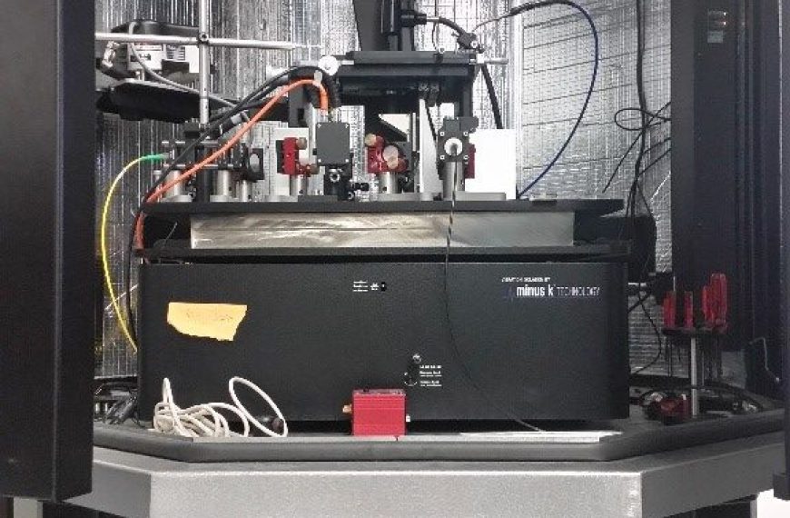
The dynamic range of the system spans DC to MHz with sub mT sensitivity for the magnetic sensing modes respectively. The imaging system is housed in a temperature-controlled and vibrationally isolated housing, which enables <0.5 K temperature stability and <5 nm drifts over the course of several hours.
Uses / Applications
Owing to the single-spin nature of the nitrogen-vacancy defect, this system is ideal for imaging emergent magnetic and transport phenomena in low dimensional materials such as skyrmions, magnons, and edge currents, with virtually no perturbation. It can also be used for the fingerprinting of integrated circuit activity, enabling measurements and characterisation of devices for energy-efficiency during testing operations as well as device tampering detection.
Specification
The system operates from 4 K to 300 K, with a 9T out-of-plane superconducting magnet, with spatial resolution of ~50 nm.
