


Description
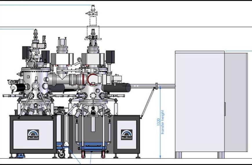
The sputtering system has numerous targets for the growth of complex metallic heterostructures for devices. The dual beam FIB-SEM system offers an alternative to the standard subtractive etch process used in optical lithography. This system can produce smaller devices without breaking vacuum, and without forming ex-situ interfaces.
Uses / Applications
Heterostructure device fabrication for a range of magnetic and optical materials systems
Specification
The AJA sputterer contains a load-lock and is configured with eleven targets, internal calibration, and automated processes. The dual-beam SEM-FIB system uses a range of ion sources including a Ga ion beam to enable direct patterning of micro- and nano-pillar devices.
