


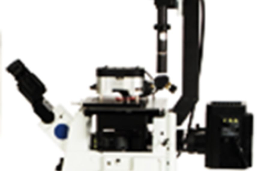
Description
The dynamic range of the system spans DC to MHz with sub mT and mK resolution for the magnetic and temperature sensing modes respectively. The imaging system is housed in a temperature-controlled and vibrationally isolated housing, which enables <0.5 K temperature stability and <5 nm drifts over the course of several hours.
Uses / Applications
The technique is non-invasive and thus enables the characterisation of surface and interface effects in highly sensitive samples with nanoscale magnetic features.
The system is also ideal for probing caloric effects in thin films and devices; mK sensitivity enables the mapping of transient heat in high bandwidth devices and circuits with nm spatial resolution, enabling measurements and characterisation of devices for energy-efficiency during testing operations under ambient conditions.
Specification
The system operates from 4 K to 300 K, with two-axis 2 T/8 T vector magnet, with spatial resolution of ~10 nm
