


Description
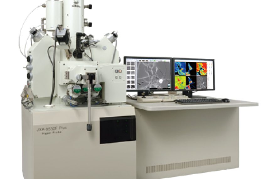
The JEOL JXA-8530F Plus Hyper Probe, is a state of the art Electron Probe Micro-analyser (EPMA) capable of performing quantitative elemental analysis of small volumes (down to 0.1µm) in solid materials.
The instrument features an In-Lens Schottky Plus Field Emission Gun (FEG) electron source optimized to provide smaller analytical probe diameters at large probe currents, of the order of micro amps, enhancing the available imaging conditions over a wide range of analytical conditions.
The FEG source provides improved secondary electron imaging resolutions: 3nm at 30kV to 50nm at 10kV. It is therefore especially suited to performing analysis at lower kV, enabling sub-micron analytical spatial resolution of fine grained features.
The instrument is equipped with 4 X-Ray spectrometers (WDS) three 2 crystal configurations and one equipped with 4 crystals providing an analytical range from Be to U.
In addition the instrument is fitted with a soft x-ray spectrometer (SXES) offering the possibility to study chemical bonding states in light elements. The JXA-8530FPlus also comes with JEOL’s 30mm2 silicon-drift detector (SDD).
A high count-rate SDD along with an in-situ variable aperture enables EDS analysis at WDS conditions allowing survey analysis particularly useful for unknown samples.
EDS spectra, maps and line scans can be acquired simultaneously with WDS data.
Equipped with a Panchromatic Cathodoluminescence (CL) system to enable high speed assessment of minute concentration differences particularly useful for the examination of minerals and mineral-like samples.
Uses / Applications
High accuracy chemical analysis and elemental mapping of a wide range of solid state materials such as defects, segregation and identification of trace elements in:
- conventional and development alloys and ceramics
- nuclear glasses
- geological materials
- archaeological artefacts
- and a whole host of potential industrial applications
Features
- Detectable element range: WDS: (Be*) / B~U,EDS: B~U
- Detectable X-ray range: Detectable wavelength range with WDS : 0.087 to 9.3nm / Detectable energy range with EDS : 20keV
- Number of spectrometers: WDS: 5, SXES: 1 EDS: 1 CL: 1
- Maximum specimen size: 100 mm × 100 mm × 50 mm (H)
- Accelerating voltage: 1 to 30 kV (0.1 kV steps)
- Probe current range: 10-12 to 5×10⁻⁷ A
- Probe current stability: ± 0.3 % /h
- Secondary electron image resolution: 3 nm (W.D. 11 mm, 30 kV)
- Minimum probe size: 40 nm (10 kV, 1×10⁻⁸ A) / 100 nm (10 kV, 1×10⁻⁷ A)
- Scanning magnification: × 40 to × 300,000 (W. D. 11 mm)
- Scanning image resolution: Maximum 5,120 × 3,840
- Large format colour display enabling easy user interface and data analysis
