


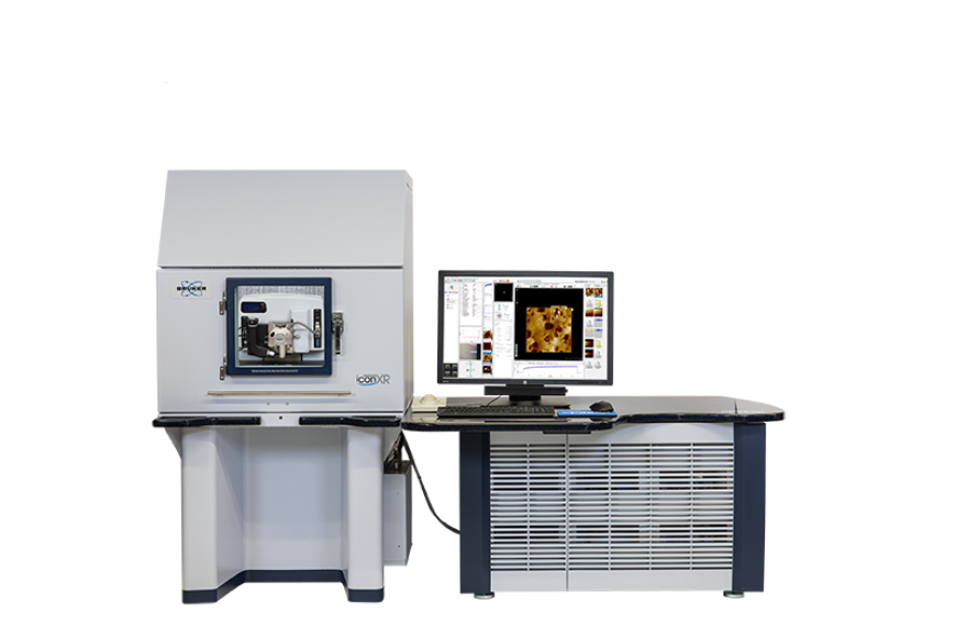
Description
Our Bruker Dimension XR AFM system is Equipped with both Icon and FastScan scan heads to deliver the utmost performance, functionality, and capability in nanoscale investigation. The Icon and FastScan platforms both excel in robust high-resolution imaging of the sample topography and nanomechanical properties with differing specifications allowing us to offer a broader range of capabilities. Additionally, each platform has unique advantages suited to various applications.
The FastScan platform offers rapid data acquisition for nanoscale imaging without compromising image resolution and force control, in both air and liquid environment. The ultimate tip-scanning speed and stability enable direct visualization of dynamic behaviours.
The Icon platform offers a comprehensive suite for advanced electrical, magnetic, piezoelectric, and electrochemical characterisations with nanometer resolution. The corresponding DataCube modes provide multidimensional information at every imaging pixel.
Specification
Max. sample size: 210mm diameter and 15mm thickness.
Max. size of a single scan: Icon Head – 90μm x 90μm with 10μm Z range; FastScan Head – 35μm x 35μm with 3μm Z range.
Working environment: Air and liquid.
In-situ optics: Top view camera.
Imaging modes: Contact Mode, Tapping Mode, ScanAsyst, PeakForce QNM and HR, Force Spectroscopy and Force Volume, FastScan, Conductive AFM (cAFM), Electrostatic Force Microscopy (EFM), Magnetic Force Microscopy (MFM), Piezo Response Microscopy (PFM), Tunneling AFM (TUNA) with DataCube (both contact and PeakForce tapping based), Kelvin Probe Force Microscopy (KPFM) (both tapping and PeakForce tapping based), Scanning Capacitance Microscopy (SCM) with Dark Lift and DataCube, Scanning Electrochemical microscopy (SECM) with DataCube.
