Atoms to Devices

The vision of our Atoms to Devices Research Area is to support the accelerated discovery and development of new device materials. Through the deposition of precisely controlled thin films, the engineering of interfaces, and the ability to control doping on the nanoscale, A2D enables the design of new devices and new technological solutions that underpin a breadth of societal applications.

Introduction and Scope

Atoms to Devices is the quantum scale engineering of new technologies, that can translate into applications ranging from photonics, imaging, semiconductors and sensors, through to energy storage, biomedical materials and quantum technologies.

The research area comprises modelling, design, growth, fabrication, characterisation, and testing of electronic, spintronic and opto-electronic devices.

The common thread that runs through the Atoms to Devices theme is the deposition of thin films, their fabrication into devices, their characterisation both chemically and structurally (XRD, Raman, XPS, EPMA) and their electrical testing, exploring the response of films exposed to electromagnetic fields from DC, through microwave and terahertz, to optical frequencies.

Current and Future Research

  • Development of electronic materials for the energy transition to meet net zero carbon targets by 2050, including research into photovoltaics, calorics and thermoelectrics, and low-loss electronics.
  • Demonstration of efficient catalysts to support carbon-free hydrogen generation.
  • Development of new device paradigms, including ‘chargeless’ electronics, new computing architectures, and quantum technologies.
  • Design of bioelectronic sensors to support personalised healthcare, and clinical assessment.
  • Development of resource abundant, scalable and recyclable materials.

Links

  • South Wales Semiconductor Cluster
  • Materials for the Energy Transition
  • Centre for Centre for Quantum Computing and Communication Technology (CQC2T)
  • UK Quantum Technology Hubs

Technology Platforms

Royce Technology Platforms are groupings of cutting-edge facilities and expertise. Each Platform has a Technology Platform Lead responsible for developing and enhancing the facilities and supporting related research activities which utilise Royce Equipment

Physical Vapour Deposition & Characterisation

The PVDC enables the growth of thin films and devices with sub-nm thickness control of individual layers, underpinning the development of advanced functional materials and devices for energy-efficient electronics.

Thin Film Device Materials

This platform provides capability for the manufacture of bespoke thin film devices, from deposition and patterning to electrical, physical, and optical characterisation, embracing the entire research and development life cycle.

Multi Chamber Deposition

The Royce Deposition System at the University of Leeds is a multi-chamber, multi-technique facility for thin film growth. Comprised of four deposition chambers connected via ultra-high vacuum transfer chambers, the Royce Deposition System allows for different deposition techniques to be combined.

Doping Materials and Device Fabrication

This platform features a novel co-beam tool utilising the implantation capabilities of a liquid metal ion source (LMIG) and the positioning accuracy of an SEM, for localised area implantation or deterministic implantation.

Atoms to Devices Team

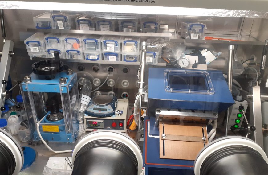
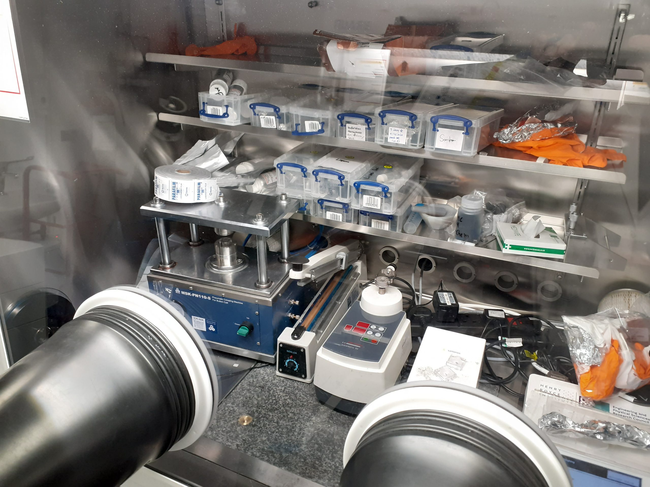
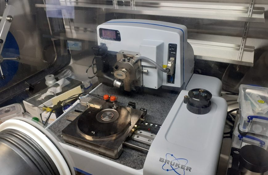
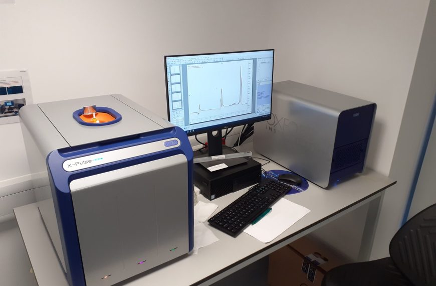
Atoms to Devices Equipment

Newsletter Signup
Privacy Overview

This website uses cookies so that we can provide you with the best user experience possible. Cookie information is stored in your browser and performs functions such as recognising you when you return to our website and helping our team to understand which sections of the website you find most interesting and useful.