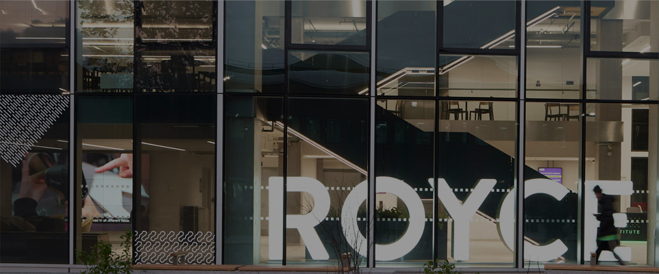


The Royce Thin Film Device Materials Platform at Imperial College London provides a platform for the manufacture of bespoke thin film devices, from deposition and patterning to electrical, physical, and optical characterisation, embracing the entire research and development life cycle.
Our unique capabilities enable users to take a thin-film device – using metals, oxides or nitrides – from conception to characterisation within two weeks as all the necessary equipment is available in our laboratories.
Our vision is to work with academic and industrial partners to realise their proof-of-principle projects and process developments in our facility, and use our consolidated knowledge and expertise to enable the next generation of exciting scientific discoveries.
The facility was originally founded by Prof Neil Alford and Dr Peter Petrov in 2001 and is open to users from both academia and industry. It is located on the 8th floor of the new, state-of-the-art Sir Michael Uren Hub based at Imperial’s White City campus.
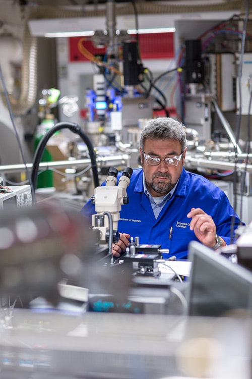
Dr Peter Petrov
Capability
Royce at the University of Sheffield combines computational material design, high-throughput materials discovery, rapid scale-up, and material property screening, to deliver a step-change in the manner novel materials are developed for specific applications.
Our capabilities support the key technical challenge of innovating processes to efficiently fabricate and test material libraries, whilst simultaneously capturing sufficient information which can be shared with manufacturers to enable rapid deployment to occur.
CE Beam Lithography Suite
Patterning
Raith E-Beam Lithographer
Yellow Room Photolithography Suite
Patterning
Karl Suss Mask Aligner
OAI Mask Aligner
Spin Coater
Cleanroom
Deposition, Patterning, Characterisation
Combined Magnetron Sputtering (HIPIMS) and E-Beam Deposition
Wide Beam Ion Milling
Inducitvely Coupled Palsma – Reactive Ion Etching
Surface Profiler
Thin Film Analyser
Deposition Lab
Deposition, Patterning, Characterisation
HEX-L Sputtering System
HEX Sputtering System
Combined Physical and Chemical Vapour Deposition
Reactive Ion Etching
Dicing Saw
Surface Profiler
Electronics Lab
Characterisation
Room Temperature Probe Station
Cryo Probe Station
RF LCR Meter
Semiconductor Device Analyser
Vector Network Analyser
Ferroelectric Test System
Current/Voltage Source and Measurement
Thermal Analyser
Preparation Lab
Preparation
1600°C Muffle Furnace
1200°C Tube Furnace
250°C Oven
Planetary Ball Mill
Target Press
Analytical Balanc
Characterisation Lab
Characterisation
MultiCore High-Performance X-ray Diffractometer
Scanning Electron Microscope
Dual beam FIB with Cyro-Stage
Laser Lab
Characterisation, Deposition
Raman Spectrometer
Atomic Force Microscope
Pulsed Laser Deposition – 4 Chambers
