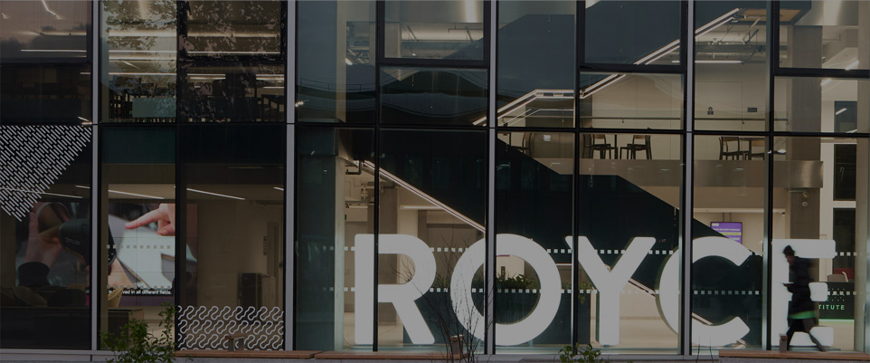


The Royce Physical Vapour Deposition and Characterisation Platform (PVDC) is hosted in the Department of Materials Science & Metallurgy at the University of Cambridge in the Centre for Materials Physics. The PVDC enables the growth of thin films and devices with sub-nm thickness control of individual layers, underpinning the development of advanced functional materials and devices for energy-efficient electronics. In particular, the facility focuses on optimising nanoscale materials and devices with targeted properties to enable low-power electronics, quantum technologies, and energy harvesting.
The PVDC includes five computer-controlled sputter deposition systems that enable the growth of up to 11 different materials in a single deposition, an ultra-high vacuum electron beam deposition system, as well as a suite of equipment to fabricate devices. This suite includes an optical mask aligner and electron beam lithography system, a focused ion beam microscope, and an atomic force microscope.

Prof. Jason Robinson
Capability
The PVDC Platform sits within the Department of Materials Science & Metallurgy at the Centre for Materials Physics and comprises a versatile set of equipment for the deposition, device fabrication and characterisation of novel materials. Equipment within in the platform provides the capability to handle samples with a thickness ranging from micrometres down to a monolayer and supports the growth of metals and insulator-thin films as well as device fabrication.
AJA Sputtering Systems
A computer-controlled growth chamber for RF and DC magnetron sputtering of thin films with sub-nm thickness control. The system has a base pressure of greater than 10−8 mbar, and enables the growth of up to 11 materials in a single deposition. Substrates with a diameter of up to 10cm can be loaded and the substrate heater, which operates at up to 850°C, enables epitaxial growth. The chamber includes an RF plasma gun for surface cleaning, a quartz crystal thickness monitor, and load lock for high-throughput fabrication of samples.
Custom Sputtering Systems
The facility includes four custom-built, highly versatile, ultra-high vacuum DC magnetron sputtering systems which enable the growth of up to five different target materials in a single deposition with automated thickness control. These systems are also set up for reactive sputtering of nitrides and non-conductive oxides.
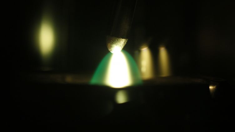
Ultra High Vacuum Electron Beam Evaporator
This five-target system can evaporate high-purity polycrystalline metallic thin films including Au, Nb, Pt, V, Al, and Cu. The system includes a quartz crystal thickness monitor, and a load lock to enable high-sample throughput.
Argon Ion Miller
This system enables anisotropic, non-selective etching of metallic and insulating thin films.
Atomic Force Microscope
A Bruker Multimode 8 with Nanoscope 5 controller with multiple modes of operation, including: contact; tapping; and peak force modes; standard atomic force microscopy; magnetic force microscopy; piezoelectric force microscopy; and Kelvin probe force microscopy.
Electron-Beam Lithography System
A LEO/ZEISS 1455VP scanning electron microscope equipped with Raith Elphy Quantum for device fabrication. The system can apply accelerating voltages from 200V to 30kV with a single write field up to 1000μm, 250nm feature resolution exposed using a 400μm write field, and PC-based pattern generator which allows up to 63 different layers.
