


Description
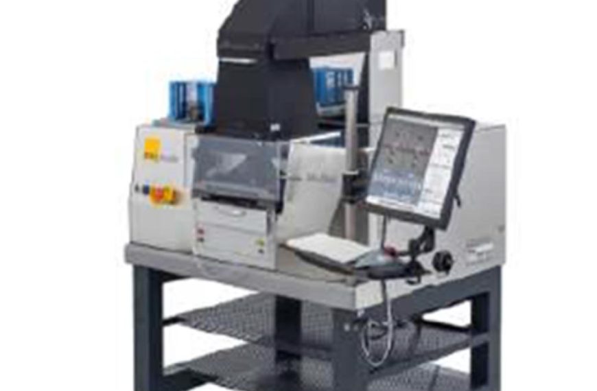
This tool represents a substantial evolution compared to previous generations, since all operations are fully automatic, with software- controlled optics and wafer chuck, which provides an automatic wafer edge compensation upon loading a substrate, as well as a video-assisted self- alignment function based on automatic pattern recognition of alignment marks.
Uses / Applications
This UV lithography tool allows the user to pattern photoresists on silicon wafers. This is a key step in any lithographic process, and may be used to fabricate, for instance, MEMS energy harvesters, microelectronic devices, and patterned electrodes for batteries or solar cells.
Specification
The UV lithography tool is the latest fourth generation Karl Suss MA6 Mask Aligner, which allows patterning of features with resolution down to approximately 700 nm, and with an alignment accuracy of 250 nm. The tool can process substrates ranging from millimetre-sized samples up to 6-inch wafers, and allows exposure in several contact modes: proximity, soft, hard, and vacuum. Furthermore, the long- focal optics are suitable for processing either thin (high-res) or thick (e.g. SU8) photoresists.
