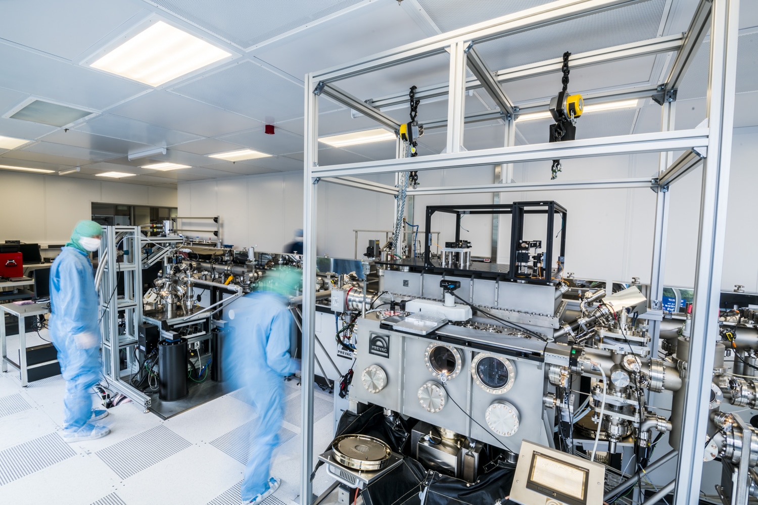
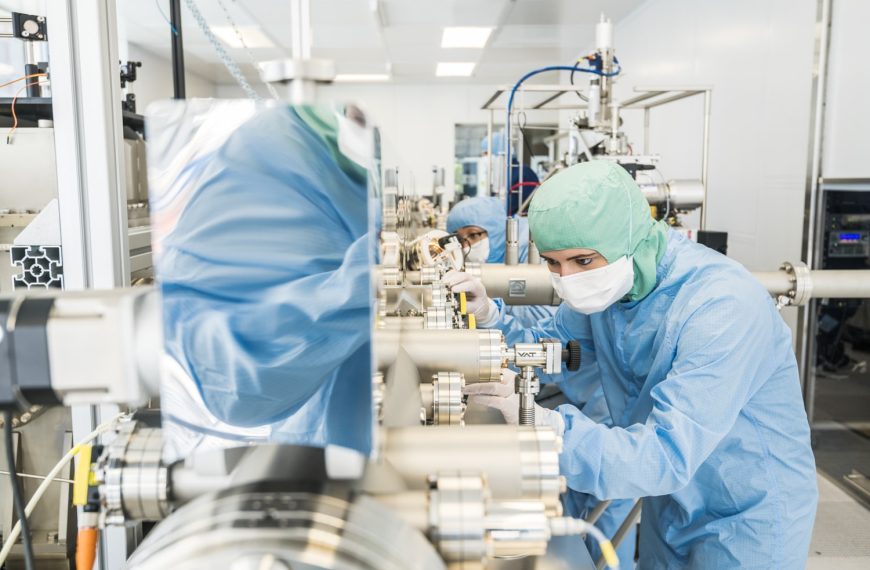
Description
LAYER BY LAYER ASSEMBLY
This chamber is the heart of the system, which allows us to isolate atomically thin materials in ultra-high vacuum granting us the unique opportunity to create devices with pristine interfaces, free from atmospheric contamination. Within the chamber, there is an in-situ optical microscopy and spectroscopy capability which can be used to identify the thickness of exfoliating crystals. Such crystals can then be assembled in a precisely chosen sequence to produce “van der Waals heterostructures”, designer solids with customisable electronic and optical properties. To perform this task “hands-free” we designed a 12-axis robotic micromanipulation setup, allowing us to stack 2D materials with an micrometer accuracy while maintaining stable temperatures up to 1000°C.
DEPOSITION
A UHV environment is ideal for producing high-quality thin films of conventional metals and insulators. The deposition chamber combines magnetron sputtering and electron beam-assisted deposition to produce electrical contacts directly onto the pristine interfaces of 2D heterostructures devices. When removed from the UHV chamber, these contacts can be used to study the electrical properties of a device. In addition, the deposition chamber has the capability for ion milling which can be used to clean or pattern devices.
SCANNING TUNNELLING MICROSCOPE
To study the surface of atomically thin crystals we use a closed cycle cryogen-free scanning tunneling microscope (STM), which is stable over a wide temperature range of 8-400K. This allows us to image the structure of 2D crystals with atomic-scale resolution, observe atomic defects and moiré superlattices. Low temperature and high stability tunneling spectroscopy also allows us to study the electronic structure of exotic 2D crystals which undergo phase transitions at low temperatures, such as magnetic ordering or Bose-Einstein condensation.