


Description
It is also used as an analysis tool to investigate the elemental composition and crystallographic structure of materials. It does this using a range of detectors that can collect electrons and x-rays emitted by excited atoms from the sample surface.
Uses / Applications
The versatility of the SEM (a large range in magnification, focal length and working distance) makes it an ideal instrument to study various characteristics of a material at the most appropriate length scale. The SEM is used to characterise fracture surfaces, grain size and morphology, and compositional differences, etc.
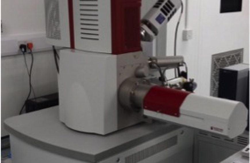
Tescan Mira XH Field Emission Gun SEM
Accelerating voltage: 200 V – 30 kV
High brightness Schottky emitter, up to 1.2 nm resolution at 30 kV
Magnification: 1x – 1,000,000x
Working distance: 2mm – 80mm
Probe current: 2 pA – 200 nA
Retracktable Backscattered Electron Detector
In-lens Secondary Electron detector for high resolution imaging
Oxford Instruments X-Max 80 for EDS characterisation
80 mm2 Silicon Drift Detector
Count rate > 500,000 cps
FWHM 129eV for MnKa
45° operating angle
AZtecEnergy software
Oxford Instruments Symmetry S2 EBSD
1244 x 1024 CCD
>4500 patterns per second
Sensitivity >800pps/nA
angular precision below 0.05 degrees
Aztec software
