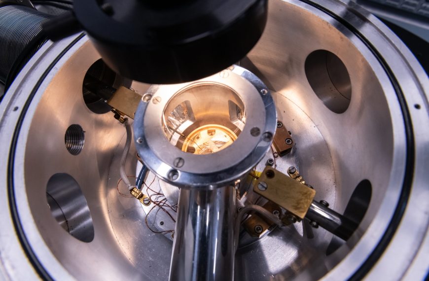
Description
The on-wafer measurements can be performed under external electrical bias and magnetic field (up to 0.15 T) applied in horizontal or vertical directions, in a wide temperature (10 K – 600 K) and frequency (d.c. – 40 GHz) ranges.
Uses / Applications
The system can be used in a wide variety of fields, including superconductivity, MEMS, ferroelectrics, nanoscale electronics, material sciences, and optics.