


Description
The Leeds Nanotechnology Cleanroom is a 800 m2 a chase-and-bay arrangement, comprising 414 m2 of equipment and processing bays, 222 m2 of clean service chase and 94 m2 of gowning and corridor, with a further 99 m2 of fallow space for future expansion. Serviced by a central corridor, the cleanroom is divided into seven rooms which broadly separate equipment into specialisation, including: Wet Etch, Dry Etch, Photolithography, Electron-beam Lithography, Metrology, Deposition, and Test and Packaging.
Capabilities
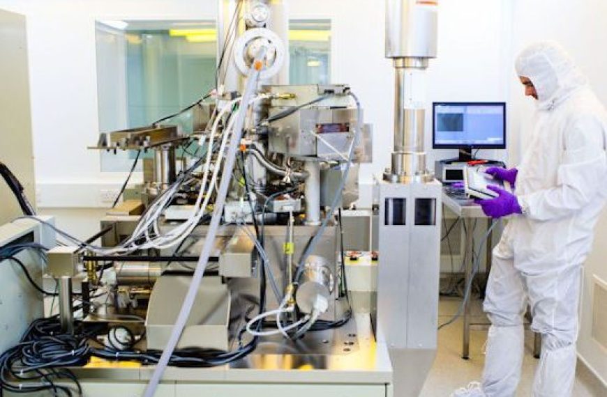
Home to our best-in-class Jeol 6300FS EBL system. This area hosts a separate control room to maintain the highest in-lab specification to allow patterning of sub-10nm structures. The room includes active field cancellation, quiet islands for the main instrument plus alignment microscopes, and advanced acoustic dampening.
Four ISO 4 (Class 10) lamina-flow wet benches for organic processing, ensuring process purity. Each bench is fitted with a dedicated spinner, DI water weir with in-built resistivity measurements, and a mixture of ultrasonic and megasonic baths for cleaning. Two stand-alone, recirculating cabinets provide PDMS processing, and temperature-controlled cold development. Equipment in this bay includes an MLA 150 maskless lithography system, an EVG 610 and two MJB 3 mask aligners, Sapphire MegPie megasonic cleaning and development system, in addition to our oxygen plasma ashers and a collection of bright-field, darkfield and DIC microscopy.
We offer a range of contact and non-contact characterisation, including using stylus profilers, AFM, optical reflectometers, 3D optical profilers and SEM imaging, all positioned on quiet islands to minimise mechanical vibrations, in addition to vibration isolation tables.
Offering PVD and CVD systems, including a sputtering system, plus three thermal and two electron-beam evaporators. This bay is also home to our wafer bonding and die bonding instruments and our rapid thermal annealer. Our CVD instruments, include an ALD for oxides and nitrides of Ti, Hf, Sn and Al; PECVD of silicon oxides, nitrides and oxynitrides; and parylene-C and parylene-N coating.
A wide range of wet and dry etching techniques are available, including ICP etching for III-V semiconductors; RIE etching of shallow silicon, silicon oxides and silicon nitrides; Ion beam etching (including CAIBE and RIBE capabilities). For wet etching, four dedicated ISO 4 lamina-flow wet benches, with integrated heated water baths for temperature control.
Offering a broad range of packaging and finishing capabilities, including lapping and polishing, dicing and scribing, alongside ribbon, ball and wedge bonding. In addition, our two probe stations and supporting electronics offer DC-to-RF characterisation capabilities.
Exact instrument specifications can be found on our equipment database: https://cleanroom.leeds.ac.uk/equipment-database/
