


Description
These equipment are part of the Electron Microscopy Centre of the Multidisciplinary Characterisation Facility.
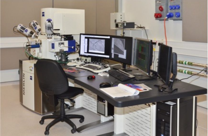
We have two advanced Scanning Electron Microscopes (SEM) the ZEISS MERLIN FEG-SEM with Oxford EBSD & EDS and the Thermofisher APREO SEM.
The Merlin has excellent beam control down to low accelerating voltages and high currents to allow some of the highest resolution characterisations of bulk materials currently possible. Incorporating both a sample exchange airlock and an integrated plasma cleaner to ensure chamber cleanliness.
Alongside the Oxford Instruments EBSD detector for crystallographic information, the Merlin is equipped with two large area EDS detectors to maximise signal collection, even at extreme beam conditions for chemical distribution mapping. In addition, a windowless EDS detector is installed that ensures characterisation capability is not lost when working at low accelerating voltages.
Electron Source
Schottky Thermal Field Emitter
Resolution @ 15 kV
0.8 nm
Resolution @ 1 kV
1.4 nm
Max. Scan Speed
25 ns/pixel
Accelerating Voltage
0.02 → 30 kV
Magnification
10× → 2,000,000×
Probe Current
10 pA → 300 nA
Image Framestore
32k × 24k pixels
Stage Type
5 axis eucentric
Stage travel
X/Y= 130 mm,
Z = 50 mm,
R = 360° Continuous,
T = -3°→ 70°
