


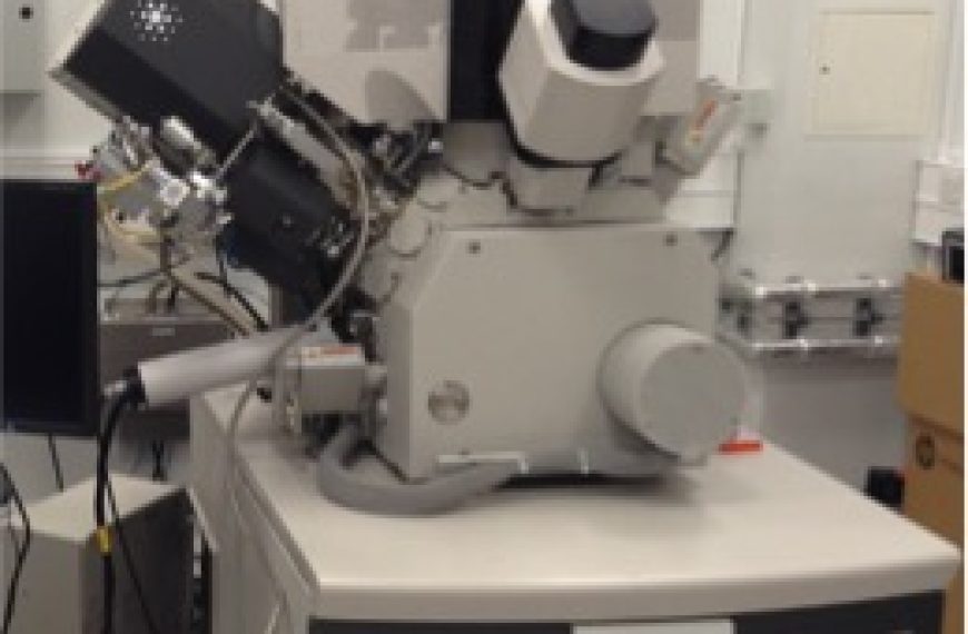
Description
This equipment is part of the Electron Microscopy Centre of the Multidisciplinary Characterisation Facility.
It is especially useful for large area high-resolution analysis. Typical applications are cross-sectional analysis, serial section 3D characterization and other large area sample preparation applications.
Uses / Applications
The ion column with powerful plasma ion source for fast milling, FEG-SEM with high-resolution for imaging, large area high-efficiency EDS detector for local elemental chemistry, and high-speed, high-precision EBSD detector for sample crystallographic analysis in one system make it a unique and versatile characterisation tool.
Electron beam
Electron beam: Dual-mode magnetic immersion / field free lens electron optics with ultra-high brightness, next-generation FEG emitter.
Source: Schottky field emitter mounted on the innovative hot-swap gun module.
Voltage: 200 V to 30 kV. Beam current: ≤22 nA. Resolution : 0.9 nm at 15 kV. 1.4 nm at 1 kV.
Ion beam: Inductively coupled plasma differentially pumped, focused ion beam optics with Xe source.
Voltage: 2 kV to 30 kV, Beam current: >1 uA in 15 steps, Resolution: 25 nm @ 30 kV.
Scanning: High-resolution digital scanning upto 6144 x 4096 pixels.
Patterning: Resolution: 64k x 64k, Pattern size: 8M pixels, Dynamically variable pixel dwell time to give 3D pattern milling.
Detectors: SE(ETD), SE/BSE(TLD), BSE(CBS), ICE.
EDS for elemental chemistry: Xmax 150 SDD detector with minimum 127eV MnKa, Oxford AZtec Energy Automated EDS, including Large Area Mapping, Map Queue.
EBSD for crystallography: NordlysMax2Fast EBSD camera, AZtecHKL Automated EBSD analysis suite, including Large Area Mapping, Map Queue, Fast Acquisition and 3D viewer software.
