Description
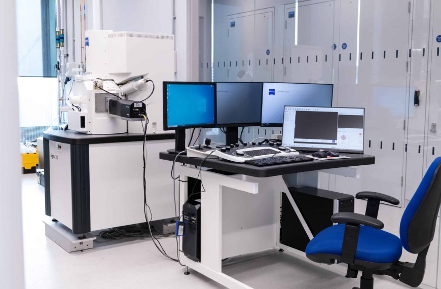
Combine field emission SEM (FE-SEM) technology with analytics. Profit from proven Gemini electron optics. Choose from a variety of detector options: image particles, surfaces, and nanostructures in materials science investigate semiconductor or medical devices, and geological or biological samples.
Save time with the semi-automated 4-step workflow of Sigma: structure your imaging and analysis routines and increase productivity. FE-SEM users of all disciplines in research and industry labs now benefit from a resolution of 1.3 nm at 1 kV in ZEISS Sigma 500 and better usability.
Uses / Applications
Imaging for thin film process control