


Description
This equipment is part of Surface Characterisation of the Multidisciplinary Characterisation Facility.
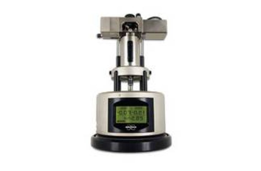
Atomic force microscopy (AFM) is an imaging technique that measures the topology of a surface with picometre height resolution. A variety of material properties may be measured simultaneously, including – notably – electrical properties (including surface potential/kelvin probe microscopy, capacitance, etc.), magnetic properties and quantitative nanomechanical properties (including modulus, adhesion, dissipation and deformation). A Peak-force TUNA (tunneling AFM) module allows for high-resolution current imaging in addition to these modes. As such, the Multimode offers versatility with a wide range of applications.
Uses / Applications
Material and Polymer Science
As a technique, AFM is uniquely well suited for investigating the nanoscale properties of nanocomposite materials.
Quantitative NanoMechanical and NanoElectrical
Fast, high-resolution mapping of nanomechanical properties including modulus over a wide range (kPa to GPa).
Biological Research
Assembled layers and functionalised surfaces.
Nanoscope V SPM controller
Application module ready
Scanner – 125 x 125 μm XY and 5 μm Z range (vertical)
Height resolution: 14 pm (last calibration)
Standard accessories
Optical microscope with 10X objective for viewing tip, sample, and laser;
Probe holder for most imaging applications in air, includes tip bias connection;
Probe holder for torsional resonance mode (TRmode);
MFM starter kit with probes and training sample;
Calibration grating for scanner calibration.
Additional accessories
Peakforce QNM technology;
STM head;
Conductive AFM application module;
Tunning AFM (TUNA) application module;
Scanning Capacitance Microscopy (SCM) module.
Maximum sample size
12 mm diameter x 5 mm thick
